

Comparison study of100A/1200V Si/SiC Hybrid IGBT Modules
Cao Lin (曹琳), Wang Fu-Zhen (王富珍),
Xi’an Yong Dian electric Co., Ltd
Abstract-In this paper a comparative study of SiC SBD in IGBT module is presented. The static and dynamic character were measured and analyzed. It is shown that the IGBT switching losses can be drastically reduced by replacing the silicon freewheeling PiN diode with SiC SBD. That enables the hybrid module more efficiency and capable of shrink the size of the power system by increasing the switching frequency. In order to explain the current and voltage oscillation during turn-on process of the hybrid module, this paper looks into the different current paths during turn-on and turn-off of the IGBT module to illustrate the conditions for oscillation. The oscillation is LC resonant that triggered by not only the stray inductance of the package but also the device capacitance in the IGBT and the freewheeling diode. Therefore, further work is necessary in low parasitic inductance package technology for SiC device, the system performance and reliability can be improved.
Keywords: IGBT module; SiC SBD; switching losses; oscillation
PACC: 2520M; 2560P; 2560H
The insulated gate bipolar transistor (IGBT) combines both the merit of MOS and bipolar structures to achieve a voltage driven power device with low on-state voltage, low switching losses and high current density, which has become the best choice for a wide range of industrial power conversion applications.
For satisfy the ever-increasing demand in power electronics applications, the designers have expended significant effort to improve system efficiency, decrease size and weight, reduce cooling equipment. All of these requirements are greatly influenced by the power dissipation that includes conduction, turn-on and turn-off losses. Lots of efforts have been done to reduce conduction and turn-off losses, such as trench field[1] stop technology and lifetime control in the buffer layer to optimize device characteristics. However, the IGBT turn-on losses are restricted depend on the freewheeling diode reverse recovery current. Thus, freewheeling diode with zero recovery charge is desirable during turn-on process.
It is shown that the superior properties enable wide bandgap silicon carbide (SiC) power devices capable of operating at higher frequencies, higher voltages, and higher temperatures. The SiC Schottky barrier diode (SBD) is now commercially available with breakdown voltage ratings of 600V-1700V and1A-60Acurrent ratings. The reverse-recovery charge in SiC SBD is extremely low and is the result of junction capacitance, not stored charge. Furthermore, unlike Si PiN ultra fast diodes, the reverse recovery character is independent on di/dt, forward current and temperature. Thus, SiC SBD as freewheeling diode in IGBT module may improving the system efficiency, lower the case temperature and reduced cooling equipment, conform IGBT module development trend.
In order to investigate the benefit of SiC SBD in IGBT module, both static and dynamic characters were measured and analyzed by comparison method in this paper. Meanwhile, the different current paths during turn-on and turn-off were analyzed in order to explain the current and voltage oscillation during hybrid module turn-on process.
In order to illustrate the benefit of SiC hybrid module, we have developed two types half-bridge module with 1200V,100Apower rating by commercially released chip. The hybrid module consists of four Si IGBT (50Aper IGBT) with eight anti-parallel SiC SBDs (20Aper diode). Another Si module consists of four Si IGBT (50Aper IGBT) with four anti-parallel Si PiN freewheeling diodes (50Aper diode). The Si IGBTs, Si PiN diodes, and the SiC SBDs are attached on the direct bond copper (DBC) substrate with minimum inductance loop. The solder joints both die and substrate, substrate and baseplate by the reflow solder systems. The top-side die contact is done with 15 mil Aluminum wires. Finally, the module is put in a plastic case filled with silicone gel for protection and insulation.
The main static characteristic of the two type module is show in table 1.
Table. 1 main static characteristic of the two type module
|
|
VGEth @25°C |
VCEsat @25°C |
VF @25°C |
VF @125°C |
ICES @25°C |
ICES @125°C |
|
Si |
5.95 V |
1.811 V |
1.797 V |
1.817 V |
0.0026 mA |
1.13 mA |
|
Hybrid |
5.94 V |
1.805 V |
1.565 V |
1.965 V |
0.0414 mA |
0.322 mA |
The gate-emitter threshold voltage (VGEth) and collector-emitter saturation voltage (VCEsat) are mainly decided by the Si IGBT chips, is nearly the same of both two type modules. Due to much low barriers, the anode-cathode on-state voltage (VF) of the SiC SBD is lower than Si PiN diode at room temperature. Meanwhile, SiC SBD exhibited strong positive temperature coefficient, is unlikely to create a current imbalance, even when multi-parallel connection. The leakage current (ICES) of the hybrid module is about 16 times larger than that of the Si module at room temperature due to low Schottky barriers. However, due to wide bandgap, there are few thermal excited carriers at high temperature, thus the leakage current of SiC SBD is less affected by temperature. The increased leakage current of hybrid module at 125 ° C is dominated by Si IGBT chips, is much less than Si module, that character enable SiC SBD operation at junction temperatures of up to 175 ° C.
The switching characters of the module were measured using a double pulse tester (DPT) with 2000μH inductive load. The self-heating of the devices is neglected due to the slow thermal time constant compared to the double pulse duration.
Compared with Si PiN diode, the main advantage of SiC SBD is its superior dynamic performance. The reverse-recovery charge in the SiC SBD is extremely low[5] and is the result of junction capacitance, not stored charge, thus best suited for fast switching application.
Figure 1 shows the measured turn-on waveform of the hybrid and Si module. The hybrid module results in a peak current (ICpk) of136A, which can be reduced significantly by 43.6% compared to the Si module.
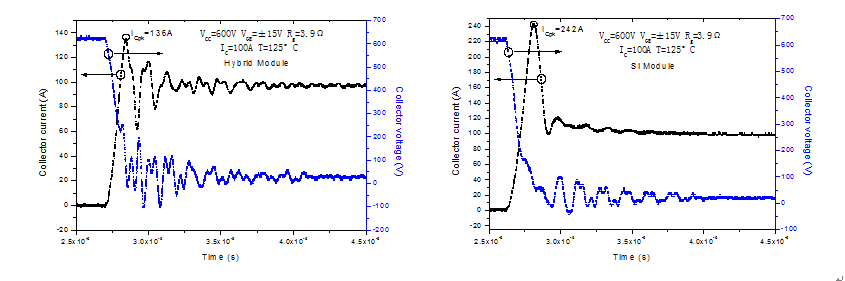
Figure 1. Turn-on waveforms of the two type IGBT module.
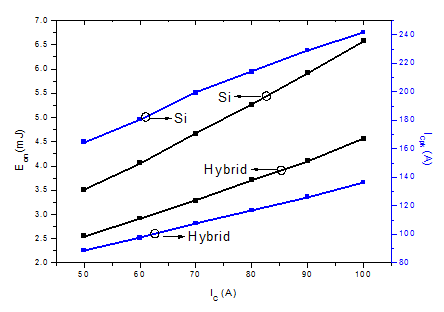
Figure 2. IGBT turn-on loss and peak current according to collector current.
The influence of the collector current on the IGBT turn-on loss and peak current can be found in figure 2. The turn-on loss is dominated by the overshoot current due to the reverse recovery charges of the freewheel diode, thus the hybrid module reduced 30.7% turn-on losses compared with Si module. The reduction in turn-on losses will improve the components efficiency and shrink the size of high power system by increasing the switching frequency.
Figure 3 shows the turn-off waveforms of the hybrid and Si module. The turn-off surge voltage (VCEpk) of the hybrid module is 25V lower than that of the Si module at100Acurrent rate. The turn-off losses of hybrid module are 7.4% lower than the Si module as figure 4 shown. In this case, the package configuration of the two type module is same, therefore the main circuit inductance are equal. The difference in the surge voltages may originate from the difference of the transient on-state voltages between SiC SBD and Si PiN diode.
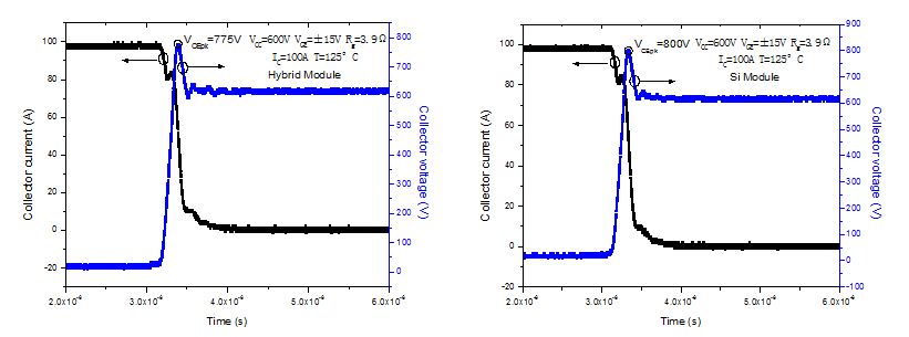
Figure 3. Turn-off waveforms of the two type IGBT module.
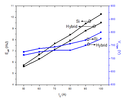
Figure 4. IGBT turn-off loss and peak current according to collector current.
The voltage and current oscillation occurred during turn-on process of the hybrid module as figure 1 shown. The IGBT switching oscillations has been discussed in some paper[8][9], and may have two possible sources. In this particular case, oscillations may come from the resonant circuit caused by the stray inductance in the package and the capacitance of the device. This section discussed the different current paths during turn-on and turn-off processes of the IGBT module for the sake of explain this particular phenomenon.
The current path during turn-on process is shown in figure 5.
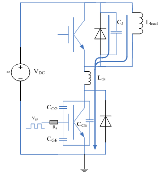
Figure 5. Current paths during turn-on process.
The turn-on oscillation occurs after the IGBT current reaches the load current as figure 1 shown. After this period, the current in the freewheeling diode is transferred to the IGBT, so the diode current decrease from its forward current (equal to load current IL) at an identical rate. After the IGBT has taken all the load current, the collector-emitter voltage (VCE) starts to fall and the freewheeling diode stops conducting, the charge store in the diode has been removed and its voltage reversed. Thus the diode junction capacitance CJ gets charged and the IGBT output capacitance COES gets discharged as figure 5 shown. Therefore the voltage and current oscillation during turn-on process should be LC-oscillation caused by the tray inductance Lds resonating with diode junction capacitance CJ and the IGBT output capacitance COES.
In the Si module of this work, the junction capacitance CJ of the PiN diode is much smaller than the IGBT output capacitance COES that is given in the datasheet. Therefore CJ in series with COES result in a capacitance close to CJ. However, in the hybrid module, due to the one decade higher critical field strength, SiC device allows two decades higher drift layer doping at the same breakdown voltage, the CJ of SiC SBD is one decade higher than Si PiN diode. Therefore, the capacitance in the hybrid module turn-on resonant circuit is much larger than Si module. This can be explaining why hybrid module exhibit more obvious oscillation than Si module.
Such an oscillation is unacceptable in the IGBT module because it’s greatly reduced reliability, possibly reduced efficiency and produced radio frequency noise. Increasing gate resistance is often effective in reducing the oscillations in the first place, but higher gate resistance also leads to increased IGBT turn-on losses, the advantages of the hybrid module were lost. Recently, Lots of work has been down to eliminates oscillation while minimizing switching losses, such as reduces the parasitic inductance in the commutation loop to suppresser the LC-resonance or ferrite bead methods. Therefore, the change from Si to SiC technology is not an easy path and lots of work must be carefully considered in the designing process of the SiC module.